Completed the data recovery work for a Lexar Professional 1667x 128GB SDXC UHS-II (U3, V60) memory card. Standard SD and SPI access was not possible, so the only viable approach was to work directly with the NAND interface. During recovery, we investigated the pinout and identified the NAND parameters. The XOR data transformation and interleave structure were successfully resolved, allowing the original data organization to be reconstructed and the user data to be accessed.
| Vendor | Samsung |
| Controller | Silicon Motion |
| Chip ID | EC1C983F84 |
| Crystals | 4 |
| Page structure | 16 x (1024 Data + 112 ECC) + 256 SA |
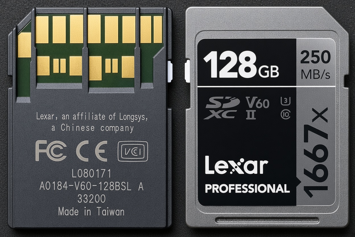
This is what the NAND interface contact-point layout of the card looks like.
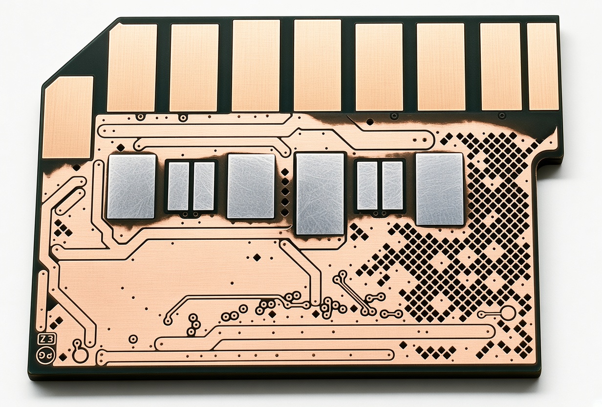
At the time of submission, no established recovery protocols existed for this particular model within major data recovery laboratories. Therefore, acquiring an identical, working donor card was essential for further investigation. The initial task involved mapping the NAND interface pinout to enable direct access to the physical storage.
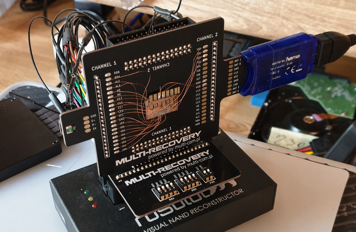
We soldered directly to the chosen contact pads and attached a logic analyzer. Once the card is powered up, the system captures the initialization/ID command and response sequence.
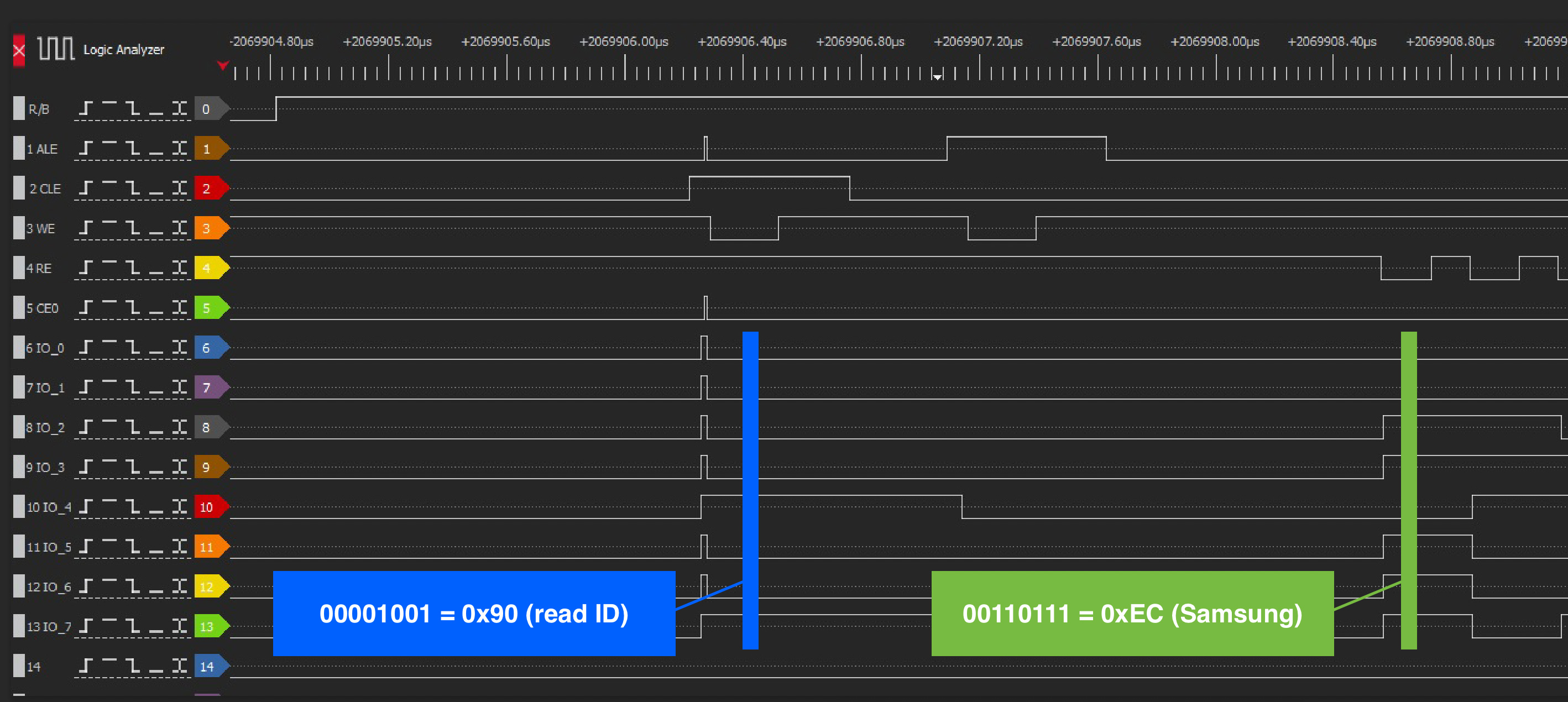
The image displays the signal waveforms for the Read ID command and the resulting response—a Samsung identifier of 0xEC. This phase of the investigation proved quite challenging. Even after correctly establishing the connections, only two of the chips could initially be read. Rusolut lab provided an X-ray scan of the card along with information on locating the two missing CE (Chip Enable) signals required to access all four chips. These additional signals were found in the fourth layer of the PCB. Reaching them required precision milling of a window into the substrate without damaging the card. This entire procedure was first prototyped and validated on the donor card.
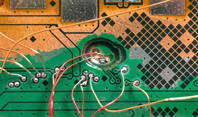
As a result, physical access to the NAND memory was achieved, yielding four 40GB raw data dumps (4x40GB). Fortunately, the card uses a standard BCH ECC algorithm, making bit error correction straightforward. The controller was identified as Silicon Motion (SM). The NAND page structure was determined through visual analysis of the bitmap.
XOR
No matching XOR key was found in the lab. To derive it, pattern data (1GB of 0x77 and 1GB of 0x00 with a 512-byte counter) was written to the donor card, allowing us to analyze data interleaving and reconstruct the key. It emerged that the XOR mask could not be directly extracted from zero-filled blocks because seven pages per block utilize a unique seed per sector. Although knowing the raw pattern allowed full XOR mask generation for the donor card, the target client card employed different initial LFSR seeds. The missing LFSR seeds for these exception pages were successfully recovered by running a full sweep of the 14-bit seed space, using JPEG MCU decoding to validate the correct values. This established the complete XOR mask for the client card.
Header & LBN

The header marker is 1 byte long and located at offset 18184, which is typical for an SM controller. Valid blocks fall within the range 0x20 to 0x3F. However, it turned out that the header value plays a crucial role in the interleaving logic. The LBN is a 32-bit little-endian integer at offset 18176, immediately followed by a second value that is exactly +1 across all pages. The purpose of this duplicate LBN remains unclear.
Interleave
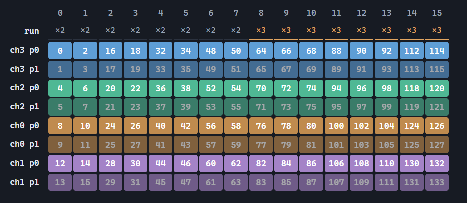
The uncovered data interleaving sequence is as follows: pairing within each chip is 1+768, and the chips are combined in the order [3,2,0,1]. However, the cycles are non-uniform; depending on the header value, 2 or 3 page pairs are taken per run.
| Page | Header | Pairs |
|---|---|---|
| 0 - 7 | 0x20 | 2 |
| 8 - 751 | 0x30 / 0x31 | 3 |
| 752 - 759 | 0x20 | 2 |
| 760 - 767 | 0x10 | service data |
The illustration below provides a visual breakdown of the interleaving logic.
Final Outcome
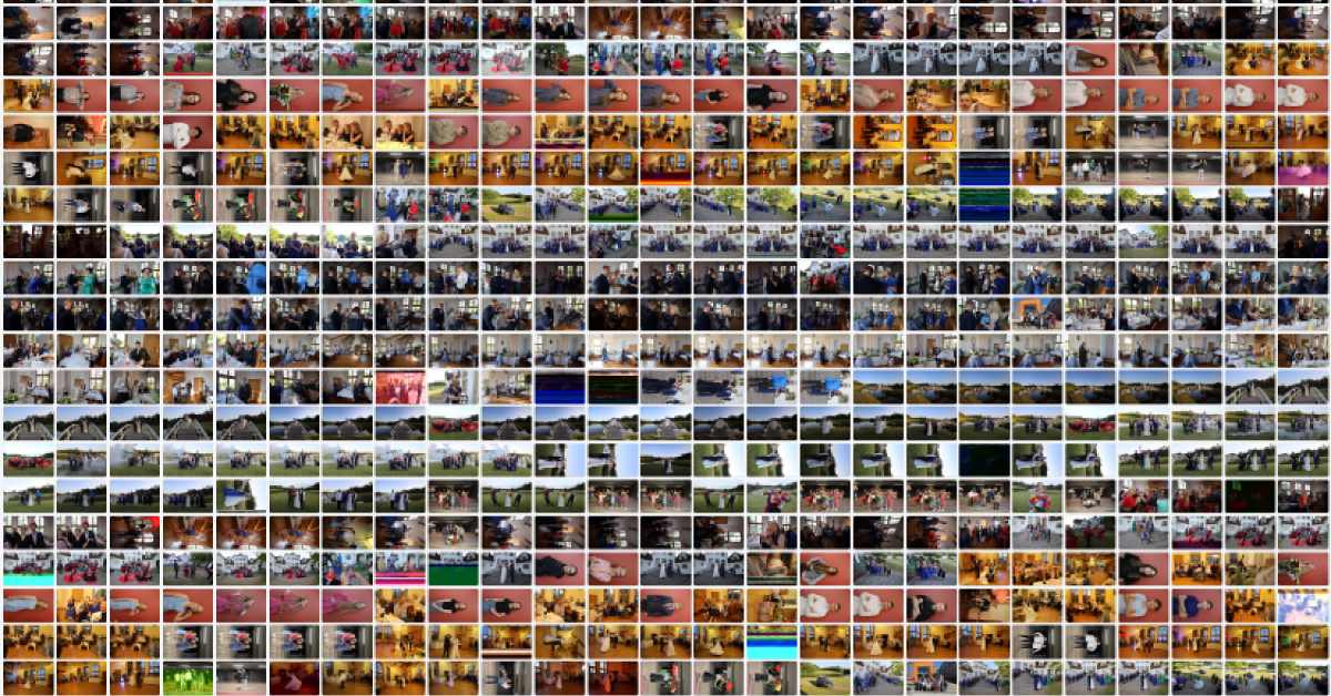
Approximately 6,300 large JPEG images (10–15 MB each) were successfully recovered from the card.